Caution: This message originated from an External Source. Use proper caution when opening attachments, clicking links, or responding.
Hi Pratap,
Thank you for the patch.
A few assorted comments to start with, I'll try to do a more in-depth
review later.
On Fri, Feb 28, 2025 at 11:53:12AM -0500, Pratap Nirujogi wrote:
Add driver for OmniVision 5.2M OV05C10 sensor. This driver
supports only the full size normal 2888x1808@30fps 2-lane
sensor profile.
What have you tested this driver with ? I see no OF device ID or ACPI
device ID.
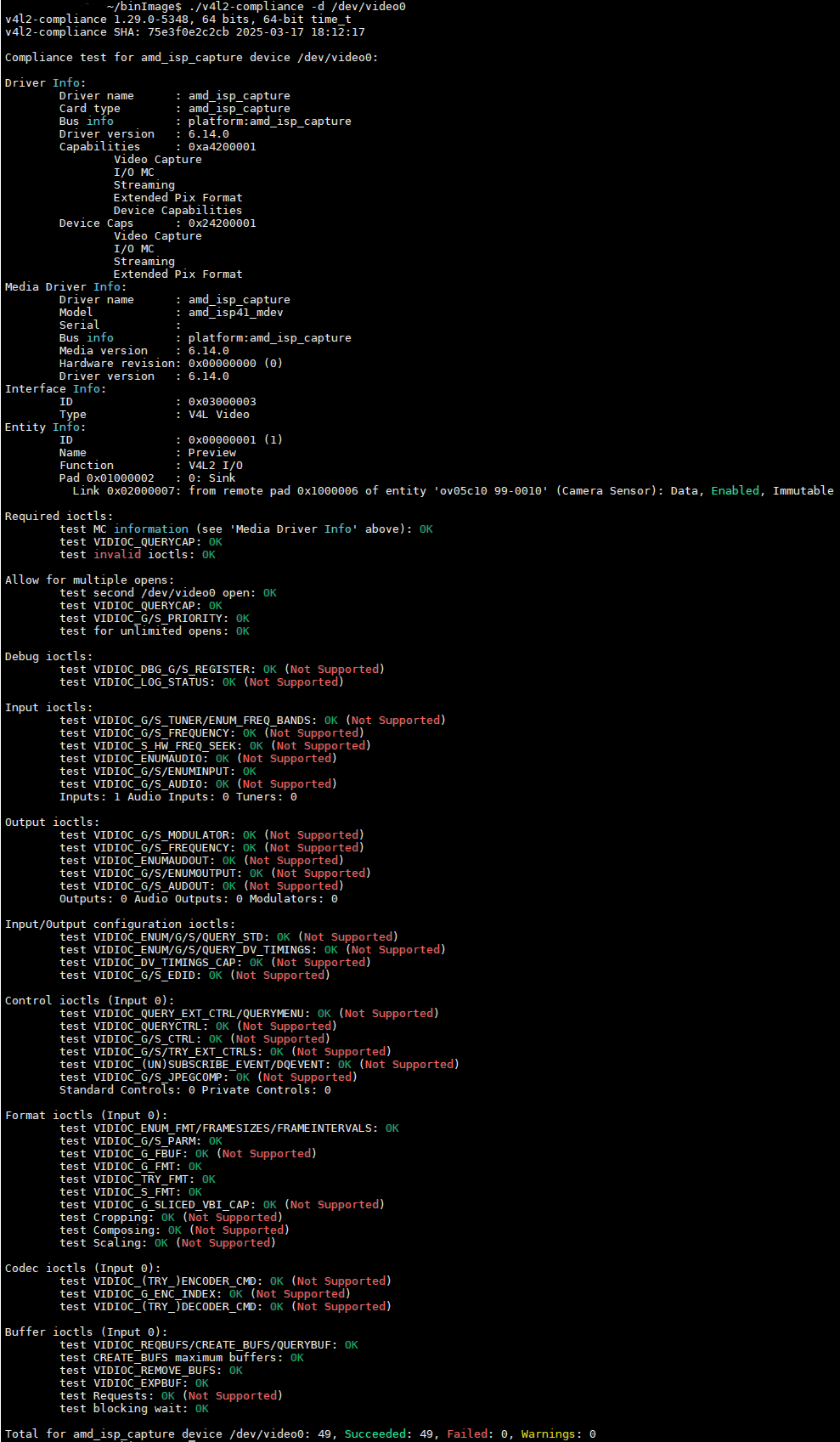
Please provide a v4l2-compliance report.
Signed-off-by: Pratap Nirujogi <pratap.nirujogi@xxxxxxx>
---
drivers/media/i2c/Kconfig | 10 +
drivers/media/i2c/Makefile | 1 +
drivers/media/i2c/ov05c.c | 1031 ++++++++++++++++++++++++++++++++++++
Please add an entry in the MAINTAINERS file.
Done. Updated in V2 patch.3 files changed, 1042 insertions(+)
create mode 100644 drivers/media/i2c/ov05c.c
diff --git a/drivers/media/i2c/Kconfig b/drivers/media/i2c/Kconfig
index 8ba096b8ebca..fd160feabc41 100644
--- a/drivers/media/i2c/Kconfig
+++ b/drivers/media/i2c/Kconfig
@@ -337,6 +337,16 @@ config VIDEO_OG01A1B
To compile this driver as a module, choose M here: the
module will be called og01a1b.
+config VIDEO_OV05C
Please sort entries alphabetically.
Done. Updated in V2 patch.+ tristate "OmniVision OV05 sensor support"
+ select V4L2_CCI_I2C
+ help
+ This is a Video4Linux2 sensor driver for the OmniVision
+ OV05C camera.
+
+ To compile this driver as a module, choose M here: the
+ module will be called OV05C.
+
config VIDEO_OV01A10
tristate "OmniVision OV01A10 sensor support"
help
diff --git a/drivers/media/i2c/Makefile b/drivers/media/i2c/Makefile
index fbb988bd067a..08bfc2d59be2 100644
--- a/drivers/media/i2c/Makefile
+++ b/drivers/media/i2c/Makefile
@@ -80,6 +80,7 @@ obj-$(CONFIG_VIDEO_MT9V011) += mt9v011.o
obj-$(CONFIG_VIDEO_MT9V032) += mt9v032.o
obj-$(CONFIG_VIDEO_MT9V111) += mt9v111.o
obj-$(CONFIG_VIDEO_OG01A1B) += og01a1b.o
+obj-$(CONFIG_VIDEO_OV05C) += ov05c.o
Here too.
Done. Updated license to GPL in V2.obj-$(CONFIG_VIDEO_OV01A10) += ov01a10.o
obj-$(CONFIG_VIDEO_OV02A10) += ov02a10.o
obj-$(CONFIG_VIDEO_OV08D10) += ov08d10.o
diff --git a/drivers/media/i2c/ov05c.c b/drivers/media/i2c/ov05c.c
new file mode 100644
index 000000000000..96c4f74af4a9
--- /dev/null
+++ b/drivers/media/i2c/ov05c.c
@@ -0,0 +1,1031 @@
+/* SPDX-License-Identifier: MIT */
Why not GPL-2.0 ?
Done. Copyright header updated as suggested.+/*
+ * Copyright (C) 2025 Advanced Micro Devices, Inc. All rights reserved.
+ * All Rights Reserved.
+ *
+ * Permission is hereby granted, free of charge, to any person obtaining a
+ * copy of this software and associated documentation files (the
+ * "Software"), to deal in the Software without restriction, including
+ * without limitation the rights to use, copy, modify, merge, publish,
+ * distribute, sub license, and/or sell copies of the Software, and to
+ * permit persons to whom the Software is furnished to do so, subject to
+ * the following conditions:
+ *
+ * The above copyright notice and this permission notice (including the
+ * next paragraph) shall be included in all copies or substantial portions
+ * of the Software.
+ *
+ * THE SOFTWARE IS PROVIDED "AS IS", WITHOUT WARRANTY OF ANY KIND, EXPRESS OR
+ * IMPLIED, INCLUDING BUT NOT LIMITED TO THE WARRANTIES OF MERCHANTABILITY,
+ * FITNESS FOR A PARTICULAR PURPOSE AND NON-INFRINGEMENT. IN NO EVENT SHALL
+ * THE COPYRIGHT HOLDERS, AUTHORS AND/OR ITS SUPPLIERS BE LIABLE FOR ANY CLAIM,
+ * DAMAGES OR OTHER LIABILITY, WHETHER IN AN ACTION OF CONTRACT, TORT OR
+ * OTHERWISE, ARISING FROM, OUT OF OR IN CONNECTION WITH THE SOFTWARE OR THE
+ * USE OR OTHER DEALINGS IN THE SOFTWARE.
Drop all this (except the copyright line), it's conveyed by the SPDX
tag.
Yes, its not used. Removed in V2.+ *
+ */
+
+#include <linux/acpi.h>
This doesn't seem to be used.
Done. Fixed the order in V2.+#include <linux/i2c.h>
+#include <linux/module.h>
+#include <linux/delay.h>
Alphabetical order please.
Those are really helpful, thank you :)+#include <linux/units.h>
+#include <linux/pm_runtime.h>
+#include <linux/gpio.h>
+#include <media/v4l2-ctrls.h>
+#include <media/v4l2-device.h>
+#include <media/v4l2-fwnode.h>
+#include <media/v4l2-cci.h>
Thanks for using the CCI helpers :-)
thank you, updated in V2.+
+#define DRV_NAME "ov05c"
+
+/* Chip ID */
+#define OV05C_REG_CHIP_ID CCI_REG24(0x00)
+#define OV05C_CHIP_ID 0x430556
+
+/* Control registers */
+#define OV05C_REG_PAGE_CTL CCI_REG8(0xFD)
V4L2 spells hex constants in lower case.
Sure, its taken care in V2.+#define OV05C_REG_TRIGGER CCI_REG8(0x01)
+
+/* V_TIMING internal */
+#define OV05C_REG_VTS CCI_REG16(0x05)
+#define OV05C_VTS_30FPS 1860
+#define OV05C_VTS_MAX 0x7fff
+
+/* H TIMING internal */
+#define OV05C_REG_HTS CCI_REG16(0x37)
+#define OV05C_HTS_30FPS 0x0280
+
+/* Exposure control */
+#define OV05C_REG_EXPOSURE CCI_REG24(0x02)
+#define OV05C_EXPOSURE_MAX_MARGIN 33
+#define OV05C_EXPOSURE_MIN 4
+#define OV05C_EXPOSURE_STEP 1
+#define OV05C_EXPOSURE_DEFAULT 0x40
+
+/* Analog gain control */
+#define OV05C_REG_ANALOG_GAIN CCI_REG8(0x24)
+#define OV05C_ANA_GAIN_MIN 0x80
+#define OV05C_ANA_GAIN_MAX 0x07c0
+#define OV05C_ANA_GAIN_STEP 1
+#define OV05C_ANA_GAIN_DEFAULT 0x80
+
+/* Digital gain control */
+#define OV05C_REG_DGTL_GAIN_H CCI_REG8(0x21)
+#define OV05C_REG_DGTL_GAIN_L CCI_REG8(0x22)
+
+#define OV05C_DGTL_GAIN_MIN 64 /* Min = 1 X */
+#define OV05C_DGTL_GAIN_MAX (256 - 1) /* Max = 4 X */
+#define OV05C_DGTL_GAIN_DEFAULT 0x80 /* Default gain = 2x */
+#define OV05C_DGTL_GAIN_STEP 1 /* Each step = 1/64 */
+
+#define OV05C_DGTL_GAIN_L_MASK 0xFF
+#define OV05C_DGTL_GAIN_H_SHIFT 8
+#define OV05C_DGTL_GAIN_H_MASK 0xFF00
+
+/* Test Pattern Control */
+#define OV05C_REG_TEST_PATTERN_CTL CCI_REG8(0xF3)
+#define OV05C_REG_TEST_PATTERN CCI_REG8(0x12)
+#define OV05C_TEST_PATTERN_ENABLE BIT(0)
Could you please sort registers by their numerical address ?
Thanks, only 1 pad is needed. Updated in V2.+
+#define NUM_OF_PADS 3
Why three pads ? The driver doesn't seem to make a distinction between
them.
Yes, its taken care in V2. We have taken care of reading the link frequency from the swnodes recently added in the latest V3 x86/platform driver patch submitted for review. The swnodes are added for this platform as the camera device specific properties in ACPI are missing.+
+enum {
+ OV05C_LINK_FREQ_900MHZ_INDEX,
+};
+
+struct ov05c_reg_list {
+ u32 num_of_regs;
+ const struct cci_reg_sequence *regs;
+};
+
+/* Link frequency config */
+struct ov05c_link_freq_config {
+ /* registers for this link frequency */
+ struct ov05c_reg_list reg_list;
+};
+
+/* Mode : resolution and related config&values */
+struct ov05c_mode {
+ /* Frame width */
+ u32 width;
+ /* Frame height */
+ u32 height;
+ /* number of lanes */
+ u32 lanes;
+
+ /* V-timing */
+ u32 vts_def;
+ u32 vts_min;
+
+ /* HTS */
+ u32 hts;
+
+ /* Index of Link frequency config to be used */
+ u32 link_freq_index;
+
+ /* Default register values */
+ struct ov05c_reg_list reg_list;
+};
+
+static const struct cci_reg_sequence
+ mode_2888_1808_30fps_1800mbps_2lane_24mhz_regs[] = {
+ { CCI_REG8(0xfd), 0x00 },
+ { CCI_REG8(0x20), 0x00 },
+ { CCI_REG8(0xfd), 0x00 },
+ { CCI_REG8(0x20), 0x0b },
+ { CCI_REG8(0xc1), 0x09 },
+ { CCI_REG8(0x21), 0x06 },
+ { CCI_REG8(0x14), 0x78 },
+ { CCI_REG8(0xe7), 0x03 },
+ { CCI_REG8(0xe7), 0x00 },
+ { CCI_REG8(0x21), 0x00 },
+ { CCI_REG8(0xfd), 0x01 },
+ { CCI_REG8(0x03), 0x00 },
+ { CCI_REG8(0x04), 0x06 },
+ { CCI_REG8(0x05), 0x07 },
+ { CCI_REG8(0x06), 0x44 },
+ { CCI_REG8(0x07), 0x08 },
+ { CCI_REG8(0x1b), 0x01 },
+ { CCI_REG8(0x24), 0xff },
+ { CCI_REG8(0x32), 0x03 },
+ { CCI_REG8(0x42), 0x5d },
+ { CCI_REG8(0x43), 0x08 },
+ { CCI_REG8(0x44), 0x81 },
+ { CCI_REG8(0x46), 0x5f },
+ { CCI_REG8(0x48), 0x18 },
+ { CCI_REG8(0x49), 0x04 },
+ { CCI_REG8(0x5c), 0x18 },
+ { CCI_REG8(0x5e), 0x13 },
+ { CCI_REG8(0x70), 0x15 },
+ { CCI_REG8(0x77), 0x35 },
+ { CCI_REG8(0x79), 0x00 },
+ { CCI_REG8(0x7b), 0x08 },
+ { CCI_REG8(0x7d), 0x08 },
+ { CCI_REG8(0x7e), 0x08 },
+ { CCI_REG8(0x7f), 0x08 },
+ { CCI_REG8(0x90), 0x37 },
+ { CCI_REG8(0x91), 0x05 },
+ { CCI_REG8(0x92), 0x18 },
+ { CCI_REG8(0x93), 0x27 },
+ { CCI_REG8(0x94), 0x05 },
+ { CCI_REG8(0x95), 0x38 },
+ { CCI_REG8(0x9b), 0x00 },
+ { CCI_REG8(0x9c), 0x06 },
+ { CCI_REG8(0x9d), 0x28 },
+ { CCI_REG8(0x9e), 0x06 },
+ { CCI_REG8(0xb2), 0x0f },
+ { CCI_REG8(0xb3), 0x29 },
+ { CCI_REG8(0xbf), 0x3c },
+ { CCI_REG8(0xc2), 0x04 },
+ { CCI_REG8(0xc4), 0x00 },
+ { CCI_REG8(0xca), 0x20 },
+ { CCI_REG8(0xcb), 0x20 },
+ { CCI_REG8(0xcc), 0x28 },
+ { CCI_REG8(0xcd), 0x28 },
+ { CCI_REG8(0xce), 0x20 },
+ { CCI_REG8(0xcf), 0x20 },
+ { CCI_REG8(0xd0), 0x2a },
+ { CCI_REG8(0xd1), 0x2a },
+ { CCI_REG8(0xfd), 0x0f },
+ { CCI_REG8(0x00), 0x00 },
+ { CCI_REG8(0x01), 0xa0 },
+ { CCI_REG8(0x02), 0x48 },
+ { CCI_REG8(0x07), 0x8f },
+ { CCI_REG8(0x08), 0x70 },
+ { CCI_REG8(0x09), 0x01 },
+ { CCI_REG8(0x0b), 0x40 },
+ { CCI_REG8(0x0d), 0x07 },
+ { CCI_REG8(0x11), 0x33 },
+ { CCI_REG8(0x12), 0x77 },
+ { CCI_REG8(0x13), 0x66 },
+ { CCI_REG8(0x14), 0x65 },
+ { CCI_REG8(0x15), 0x37 },
+ { CCI_REG8(0x16), 0xbf },
+ { CCI_REG8(0x17), 0xff },
+ { CCI_REG8(0x18), 0xff },
+ { CCI_REG8(0x19), 0x12 },
+ { CCI_REG8(0x1a), 0x10 },
+ { CCI_REG8(0x1c), 0x77 },
+ { CCI_REG8(0x1d), 0x77 },
+ { CCI_REG8(0x20), 0x0f },
+ { CCI_REG8(0x21), 0x0f },
+ { CCI_REG8(0x22), 0x0f },
+ { CCI_REG8(0x23), 0x0f },
+ { CCI_REG8(0x2b), 0x20 },
+ { CCI_REG8(0x2c), 0x20 },
+ { CCI_REG8(0x2d), 0x04 },
+ { CCI_REG8(0xfd), 0x03 },
+ { CCI_REG8(0x9d), 0x0f },
+ { CCI_REG8(0x9f), 0x40 },
+ { CCI_REG8(0xfd), 0x00 },
+ { CCI_REG8(0x20), 0x1b },
+ { CCI_REG8(0xfd), 0x04 },
+ { CCI_REG8(0x19), 0x60 },
+ { CCI_REG8(0xfd), 0x02 },
+ { CCI_REG8(0x75), 0x05 },
+ { CCI_REG8(0x7f), 0x06 },
+ { CCI_REG8(0x9a), 0x03 },
+ { CCI_REG8(0xa2), 0x07 },
+ { CCI_REG8(0xa3), 0x10 },
+ { CCI_REG8(0xa5), 0x02 },
+ { CCI_REG8(0xa6), 0x0b },
+ { CCI_REG8(0xa7), 0x48 },
+ { CCI_REG8(0xfd), 0x07 },
+ { CCI_REG8(0x42), 0x00 },
+ { CCI_REG8(0x43), 0x80 },
+ { CCI_REG8(0x44), 0x00 },
+ { CCI_REG8(0x45), 0x80 },
+ { CCI_REG8(0x46), 0x00 },
+ { CCI_REG8(0x47), 0x80 },
+ { CCI_REG8(0x48), 0x00 },
+ { CCI_REG8(0x49), 0x80 },
+ { CCI_REG8(0x00), 0xf7 },
+ { CCI_REG8(0xfd), 0x00 },
+ { CCI_REG8(0xe7), 0x03 },
+ { CCI_REG8(0xe7), 0x00 },
+ { CCI_REG8(0xfd), 0x00 },
+ { CCI_REG8(0x93), 0x18 },
+ { CCI_REG8(0x94), 0xff },
+ { CCI_REG8(0x95), 0xbd },
+ { CCI_REG8(0x96), 0x1a },
+ { CCI_REG8(0x98), 0x04 },
+ { CCI_REG8(0x99), 0x08 },
+ { CCI_REG8(0x9b), 0x10 },
+ { CCI_REG8(0x9c), 0x3f },
+ { CCI_REG8(0xa1), 0x05 },
+ { CCI_REG8(0xa4), 0x2f },
+ { CCI_REG8(0xc0), 0x0c },
+ { CCI_REG8(0xc1), 0x08 },
+ { CCI_REG8(0xc2), 0x00 },
+ { CCI_REG8(0xb6), 0x20 },
+ { CCI_REG8(0xbb), 0x80 },
+ { CCI_REG8(0xfd), 0x00 },
+ { CCI_REG8(0xa0), 0x01 },
+ { CCI_REG8(0xfd), 0x01 },
+};
+
+static const struct cci_reg_sequence mode_OV05C_stream_on_regs[] = {
+ { CCI_REG8(0xfd), 0x01 },
+ { CCI_REG8(0x33), 0x03 },
+ { CCI_REG8(0x01), 0x02 },
+ { CCI_REG8(0xfd), 0x00 },
+ { CCI_REG8(0x20), 0x1f },
+ { CCI_REG8(0xfd), 0x01 },
+};
+
+static const struct cci_reg_sequence mode_OV05C_stream_off_regs[] = {
+ { CCI_REG8(0xfd), 0x00 },
+ { CCI_REG8(0x20), 0x5b },
+ { CCI_REG8(0xfd), 0x01 },
+ { CCI_REG8(0x33), 0x02 },
+ { CCI_REG8(0x01), 0x02 },
+};
+
+static const char * const ov05c_test_pattern_menu[] = {
+ "Disabled",
+ "Vertical Color Bar Type 1",
+ "Vertical Color Bar Type 2",
+ "Vertical Color Bar Type 3",
+ "Vertical Color Bar Type 4"
+};
+
+/* Configurations for supported link frequencies */
+#define OV05C_LINK_FREQ_900MHZ (900 * HZ_PER_MHZ)
+
+/* Number of lanes supported */
+#define OV05C_DATA_LANES 2
+
+/* Bits per sample of sensor output */
+#define OV05C_BITS_PER_SAMPLE 10
+
+/*
+ * pixel_rate = link_freq * data-rate * nr_of_lanes / bits_per_sample
+ * data rate => double data rate; number of lanes => 2; bits per pixel => 10
+ */
+static u64 link_freq_to_pixel_rate(u64 f)
+{
+ f *= 2 * OV05C_DATA_LANES;
+ do_div(f, OV05C_BITS_PER_SAMPLE);
+
+ return f;
+}
+
+/* Menu items for LINK_FREQ V4L2 control */
+static const s64 ov05c_link_freq_menu_items[] = {
+ OV05C_LINK_FREQ_900MHZ,
+};
The link frequencies should be parsed from device properties (DT or
ACPI), not be hardcoded in the driver. PLL parameters should be computed
dynamically accordingly.
Ideally its possible, but for this particular sensor we have register settings only for this mode from the vendor.+
+/* Mode configs */
+static const struct ov05c_mode supported_modes[] = {
+ {
+ .width = 2888,
+ .height = 1808,
Can the sensor registers related to the image size be set based on the
format set by userspace, instead of hardcoding modes ?
We found this mutex is not required and removed it in V2.+ .vts_def = OV05C_VTS_30FPS,
+ .vts_min = OV05C_VTS_30FPS,
+ .hts = 640,
+ .lanes = 2,
+ .reg_list = {
+ .num_of_regs = ARRAY_SIZE(mode_2888_1808_30fps_1800mbps_2lane_24mhz_regs),
+ .regs = mode_2888_1808_30fps_1800mbps_2lane_24mhz_regs,
+ },
+ .link_freq_index = OV05C_LINK_FREQ_900MHZ_INDEX,
+ },
+};
+
+struct ov05c {
+ struct v4l2_subdev sd;
+ struct media_pad pads[NUM_OF_PADS];
+
+ /* V4L2 control handler */
+ struct v4l2_ctrl_handler ctrl_handler;
+
+ /* V4L2 Controls */
+ struct v4l2_ctrl *link_freq;
+ struct v4l2_ctrl *pixel_rate;
+ struct v4l2_ctrl *vblank;
+ struct v4l2_ctrl *hblank;
+ struct v4l2_ctrl *exposure;
+
+ /* Current mode */
+ const struct ov05c_mode *cur_mode;
+
+ struct regmap *regmap;
+
+ /* Mutex for serialized access */
You need to document which fields the mutex protects.
Done. Removed open() and added init_state() in V2.+ struct mutex mutex;
+
+ /* gpio descriptor */
+ struct gpio_desc *enable_gpio;
+};
+
+#define to_ov05c(_sd) container_of(_sd, struct ov05c, sd)
+
+static int ov05c_open(struct v4l2_subdev *sd, struct v4l2_subdev_fh *fh)
.open() is normally not used for sensor drivers. You should use
.init_state() instead.
thanks for this suggestion. We have taken care of it in V2.+{
+ const struct ov05c_mode *default_mode = &supported_modes[0];
+ struct ov05c *ov05c = to_ov05c(sd);
+ struct v4l2_mbus_framefmt *try_fmt =
+ v4l2_subdev_state_get_format(fh->state, 0);
+
+ mutex_lock(&ov05c->mutex);
+
+ /* Initialize try_fmt */
+ try_fmt->width = default_mode->width;
+ try_fmt->height = default_mode->height;
+ try_fmt->code = MEDIA_BUS_FMT_SGRBG10_1X10;
+ try_fmt->field = V4L2_FIELD_NONE;
+
+ /* No crop or compose */
+ mutex_unlock(&ov05c->mutex);
+
+ return 0;
+}
+
+static int ov05c_update_cid_vblank(struct ov05c *ov05c, u32 vblank)
+{
+ int ret = 0;
+
+ cci_write(ov05c->regmap, OV05C_REG_PAGE_CTL,
Controlling the page manually is error-prone. Could you encode the page
number in the register address, and implement read/write wrapper
functions that will set the page and call cci_read() and cci_write() ?
You can then cache the active page, and avoid writing OV05C_REG_PAGE_CTL
unnecessarily?
Done. Removed in V2.+ BIT(0), &ret);
+ if (ret)
+ return ret;
Drop this, and ...
+
+ cci_write(ov05c->regmap, OV05C_REG_VTS,
+ ov05c->cur_mode->height
+ + vblank, &ret);
+ if (ret)
+ return ret;
drop this too ...
sure, added macro OV05C_REG_TRIGGER_START in V2.+
+ cci_write(ov05c->regmap, OV05C_REG_TRIGGER,
+ BIT(0), &ret);
Please create macros for register bits.
Refactored ov05c10_update control funcs. Please see V2 and let us know your opinion.+
+ return ret;
and the function will behave as you expect. If ret is not zero,
cci_write() returns immediately, so you can have multiple cci_write()
calls without intermediate error handling. The same applies everywhere
in the driver.
thanks, implemented in V2.+}
+
+static int ov05c_update_cid_exposure(struct ov05c *ov05c, u32 exposure)
+{
+ int ret = 0;
+
+ cci_write(ov05c->regmap, OV05C_REG_PAGE_CTL,
+ BIT(0), &ret);
+ if (ret)
+ return ret;
+
+ cci_write(ov05c->regmap, OV05C_REG_EXPOSURE,
+ exposure, &ret);
+ if (ret)
+ return ret;
+
+ cci_write(ov05c->regmap, OV05C_REG_TRIGGER,
+ BIT(0), &ret);
+
+ return ret;
+}
+
+static int ov05c_update_analog_gain(struct ov05c *ov05c, u32 a_gain)
+{
+ int ret;
+
+ ret = cci_write(ov05c->regmap, OV05C_REG_PAGE_CTL, BIT(0), NULL);
+ if (ret)
+ return ret;
+
+ ret = cci_write(ov05c->regmap, OV05C_REG_ANALOG_GAIN, a_gain, NULL);
+ if (ret)
+ return ret;
+
+ return cci_write(ov05c->regmap, OV05C_REG_TRIGGER, BIT(0), NULL);
+}
+
+static int ov05_update_digital_gain(struct ov05c *ov05c, u32 d_gain)
+{
+ int ret;
+ u64 val;
+
+ ret = cci_write(ov05c->regmap, OV05C_REG_PAGE_CTL, BIT(0), NULL);
+ if (ret)
+ return ret;
+
+ val = d_gain & OV05C_DGTL_GAIN_L_MASK;
+ ret = cci_write(ov05c->regmap, OV05C_REG_DGTL_GAIN_L, val, NULL);
+ if (ret)
+ return ret;
+
+ val = (d_gain & OV05C_DGTL_GAIN_H_MASK) >> OV05C_DGTL_GAIN_H_SHIFT;
+
+ ret = cci_write(ov05c->regmap, OV05C_REG_DGTL_GAIN_H, val, NULL);
+ if (ret)
+ return ret;
+
+ return cci_write(ov05c->regmap, OV05C_REG_TRIGGER, BIT(0), NULL);
+}
+
+static int ov05c_enable_test_pattern(struct ov05c *ov05c, u32 pattern)
+{
+ int ret;
+ u64 val;
+
+ ret = cci_write(ov05c->regmap, OV05C_REG_PAGE_CTL, BIT(2), NULL);
+ if (ret)
+ return ret;
+
+ if (pattern) {
+ ret = cci_read(ov05c->regmap, OV05C_REG_TEST_PATTERN_CTL, &val, NULL);
+ if (ret)
+ return ret;
+
+ ret = cci_write(ov05c->regmap, OV05C_REG_TEST_PATTERN_CTL, val | BIT(1), NULL);
+ if (ret)
+ return ret;
+
+ ret = cci_read(ov05c->regmap, OV05C_REG_TEST_PATTERN, &val, NULL);
+ if (ret)
+ return ret;
+
+ val &= OV05C_TEST_PATTERN_ENABLE;
+ } else {
+ ret = cci_read(ov05c->regmap, OV05C_REG_TEST_PATTERN, &val, NULL);
+ if (ret)
+ return ret;
+
+ val &= ~OV05C_TEST_PATTERN_ENABLE;
+ }
+
+ ret = cci_write(ov05c->regmap, OV05C_REG_TEST_PATTERN, val, NULL);
+ if (ret)
+ return ret;
+
+ return cci_write(ov05c->regmap, OV05C_REG_TRIGGER, BIT(0), NULL);
+}
+
+static int ov05c_set_ctrl(struct v4l2_ctrl *ctrl)
+{
+ struct ov05c *ov05c = container_of(ctrl->handler,
+ struct ov05c, ctrl_handler);
+ struct i2c_client *client = v4l2_get_subdevdata(&ov05c->sd);
+ s64 max;
+ int ret = 0;
+
+ /* Propagate change of current control to all related controls */
+ switch (ctrl->id) {
+ case V4L2_CID_VBLANK:
+ /* Update max exposure while meeting expected vblanking */
+ max = ov05c->cur_mode->height + ctrl->val - OV05C_EXPOSURE_MAX_MARGIN;
+ __v4l2_ctrl_modify_range(ov05c->exposure,
+ ov05c->exposure->minimum,
+ max, ov05c->exposure->step, max);
+ break;
+ }
+
+ /*
+ * Applying V4L2 control value only happens
+ * when power is up for streaming
+ */
+ if (!pm_runtime_get_if_in_use(&client->dev))
+ return 0;
+
+ switch (ctrl->id) {
+ case V4L2_CID_ANALOGUE_GAIN:
+ ret = ov05c_update_analog_gain(ov05c, ctrl->val);
+ break;
+ case V4L2_CID_DIGITAL_GAIN:
+ ret = ov05_update_digital_gain(ov05c, ctrl->val);
+ break;
+ case V4L2_CID_EXPOSURE:
+ ret = ov05c_update_cid_exposure(ov05c, ctrl->val);
+ break;
+ case V4L2_CID_VBLANK:
+ ret = ov05c_update_cid_vblank(ov05c, ctrl->val);
+ break;
+ case V4L2_CID_TEST_PATTERN:
+ ret = ov05c_enable_test_pattern(ov05c, ctrl->val);
+ break;
+ default:
+ dev_info(&client->dev,
+ "ctrl(id:0x%x,val:0x%x) is not handled\n",
+ ctrl->id, ctrl->val);
+ break;
+ }
+
+ pm_runtime_put(&client->dev);
+
+ return ret;
+}
+
+static const struct v4l2_ctrl_ops ov05c_ctrl_ops = {
+ .s_ctrl = ov05c_set_ctrl,
+};
+
+static int ov05c_enum_mbus_code(struct v4l2_subdev *sd,
+ struct v4l2_subdev_state *sd_state,
+ struct v4l2_subdev_mbus_code_enum *code)
+{
+ /* Only one bayer order(GRBG) is supported */
+ if (code->index > 0)
+ return -EINVAL;
+
+ code->code = MEDIA_BUS_FMT_SGRBG10_1X10;
+
+ return 0;
+}
+
+static int ov05c_enum_frame_size(struct v4l2_subdev *sd,
+ struct v4l2_subdev_state *sd_state,
+ struct v4l2_subdev_frame_size_enum *fse)
+{
+ if (fse->index >= ARRAY_SIZE(supported_modes))
+ return -EINVAL;
+
+ if (fse->code != MEDIA_BUS_FMT_SGRBG10_1X10)
+ return -EINVAL;
+
+ fse->min_width = supported_modes[fse->index].width;
+ fse->max_width = fse->min_width;
+ fse->min_height = supported_modes[fse->index].height;
+ fse->max_height = fse->min_height;
+
+ return 0;
+}
+
+static void ov05c_update_pad_format(const struct ov05c_mode *mode,
+ struct v4l2_subdev_format *fmt)
+{
+ fmt->format.width = mode->width;
+ fmt->format.height = mode->height;
+ fmt->format.code = MEDIA_BUS_FMT_SGRBG10_1X10;
+ fmt->format.field = V4L2_FIELD_NONE;
+}
+
+static int ov05c_do_get_pad_format(struct ov05c *ov05c,
+ struct v4l2_subdev_state *sd_state,
+ struct v4l2_subdev_format *fmt)
+{
+ struct v4l2_mbus_framefmt *framefmt;
+
+ if (fmt->which == V4L2_SUBDEV_FORMAT_TRY) {
+ framefmt = v4l2_subdev_state_get_format(sd_state, fmt->pad);
+ fmt->format = *framefmt;
+ } else {
+ ov05c_update_pad_format(ov05c->cur_mode, fmt);
+ }
+
+ return 0;
+}
+
+static int ov05c_get_pad_format(struct v4l2_subdev *sd,
+ struct v4l2_subdev_state *sd_state,
+ struct v4l2_subdev_format *fmt)
+{
+ struct ov05c *ov05c = to_ov05c(sd);
+ int ret;
+
+ mutex_lock(&ov05c->mutex);
+ ret = ov05c_do_get_pad_format(ov05c, sd_state, fmt);
+ mutex_unlock(&ov05c->mutex);
+
+ return ret;
+}
+
+static int ov05c_set_pad_format(struct v4l2_subdev *sd,
+ struct v4l2_subdev_state *sd_state,
+ struct v4l2_subdev_format *fmt)
+{
+ struct ov05c *ov05c = to_ov05c(sd);
+ const struct ov05c_mode *mode;
+ struct v4l2_mbus_framefmt *framefmt;
+ s32 vblank_def;
+ s32 vblank_min;
+ s64 h_blank;
+ s64 pixel_rate;
+ s64 link_freq;
+
+ mutex_lock(&ov05c->mutex);
+
+ /* Only one raw bayer(GRBG) order is supported */
+ if (fmt->format.code != MEDIA_BUS_FMT_SGRBG10_1X10)
+ fmt->format.code = MEDIA_BUS_FMT_SGRBG10_1X10;
+
+ mode = v4l2_find_nearest_size(supported_modes,
+ ARRAY_SIZE(supported_modes),
+ width, height,
+ fmt->format.width, fmt->format.height);
+ ov05c_update_pad_format(mode, fmt);
+ if (fmt->which == V4L2_SUBDEV_FORMAT_TRY) {
+ framefmt = v4l2_subdev_state_get_format(sd_state, fmt->pad);
+ *framefmt = fmt->format;
+ } else {
+ ov05c->cur_mode = mode;
+ __v4l2_ctrl_s_ctrl(ov05c->link_freq, mode->link_freq_index);
+ link_freq = ov05c_link_freq_menu_items[mode->link_freq_index];
+ pixel_rate = link_freq_to_pixel_rate(link_freq);
+ __v4l2_ctrl_s_ctrl_int64(ov05c->pixel_rate, pixel_rate);
+
+ /* Update limits and set FPS to default */
+ vblank_def = ov05c->cur_mode->vts_def -
+ ov05c->cur_mode->height;
+ vblank_min = ov05c->cur_mode->vts_min -
+ ov05c->cur_mode->height;
+ __v4l2_ctrl_modify_range(ov05c->vblank, vblank_min,
+ OV05C_VTS_MAX
+ - ov05c->cur_mode->height,
+ 1,
+ vblank_def);
+ __v4l2_ctrl_s_ctrl(ov05c->vblank, vblank_def);
+ h_blank = ov05c->cur_mode->hts;
+ __v4l2_ctrl_modify_range(ov05c->hblank, h_blank,
+ h_blank, 1, h_blank);
+ }
+
+ mutex_unlock(&ov05c->mutex);
+
+ return 0;
+}
+
+static int ov05c_start_streaming(struct ov05c *ov05c)
+{
+ struct i2c_client *client = v4l2_get_subdevdata(&ov05c->sd);
+ const struct ov05c_reg_list *reg_list;
+ int ret = 0;
+
+ /* Apply default values of current mode */
+ reg_list = &ov05c->cur_mode->reg_list;
+ cci_multi_reg_write(ov05c->regmap, reg_list->regs, reg_list->num_of_regs,
+ &ret);
+ if (ret) {
+ dev_err(&client->dev, "%s failed to set mode, ret: %d\n", __func__, ret);
+ return ret;
+ }
+
+ /* Apply customized values from user */
+ ret = __v4l2_ctrl_handler_setup(ov05c->sd.ctrl_handler);
+ if (ret) {
+ dev_err(&client->dev, "__v4l2_ctrl_handler_setup err:%d", ret);
+ return ret;
+ }
+
+ cci_multi_reg_write(ov05c->regmap, mode_OV05C_stream_on_regs,
+ ARRAY_SIZE(mode_OV05C_stream_on_regs), &ret);
+ if (ret)
+ dev_err(&client->dev, "%s failed to start the streaming\n", __func__);
+
+ return ret;
+}
+
+static int ov05c_stop_streaming(struct ov05c *ov05c)
+{
+ int ret = 0;
+ struct i2c_client *client = v4l2_get_subdevdata(&ov05c->sd);
+
+ cci_multi_reg_write(ov05c->regmap, mode_OV05C_stream_off_regs,
+ ARRAY_SIZE(mode_OV05C_stream_off_regs), &ret);
+ if (ret)
+ dev_err(&client->dev, "%s failed to stop the streaming\n", __func__);
+
+ return ret;
+}
+
+static void ov05c_sensor_enable(struct ov05c *ov05c, bool enable)
+{
+ if (enable) {
+ gpiod_set_value(ov05c->enable_gpio, 0);
+ usleep_range(10, 20);
+
+ gpiod_set_value(ov05c->enable_gpio, 1);
+ /* The delay is to make sure the sensor is completely turned on */
+ usleep_range(1000, 2000);
+ } else {
+ gpiod_set_value(ov05c->enable_gpio, 0);
+ usleep_range(10, 20);
+ }
+}
+
+static int ov05c_set_stream(struct v4l2_subdev *sd, int enable)
+{
+ struct ov05c *ov05c = to_ov05c(sd);
+ struct i2c_client *client = v4l2_get_subdevdata(sd);
+ int ret = 0;
+
+ mutex_lock(&ov05c->mutex);
+
+ if (enable) {
+ ov05c_sensor_enable(ov05c, true);
+
+ ret = pm_runtime_resume_and_get(&client->dev);
+ if (ret < 0)
+ goto err_unlock;
+
+ /*
+ * Apply default & customized values
+ * and then start streaming.
+ */
+ ret = ov05c_start_streaming(ov05c);
+ if (ret)
+ goto err_rpm_put;
+ } else {
+ ov05c_stop_streaming(ov05c);
+ pm_runtime_put(&client->dev);
+
+ ov05c_sensor_enable(ov05c, false);
+ }
+
+ mutex_unlock(&ov05c->mutex);
+
+ return ret;
+
+err_rpm_put:
+ pm_runtime_put(&client->dev);
+err_unlock:
+ mutex_unlock(&ov05c->mutex);
+
+ return ret;
+}
+
+static const struct v4l2_subdev_video_ops ov05c_video_ops = {
+ .s_stream = ov05c_set_stream,
Please implement the .enable_streams() and .disable_streams() operations
instead.
thanks, replaced ov05c_get_pad_format() with v4l2_subdev_get_fmt() in V2.+};
+
+static const struct v4l2_subdev_pad_ops ov05c_pad_ops = {
+ .enum_mbus_code = ov05c_enum_mbus_code,
+ .get_fmt = ov05c_get_pad_format,
Use v4l2_subdev_get_fmt() here and drop the manual implementation of
ov05c_get_pad_format(). You will need to call
v4l2_subdev_init_finalize() at probe time. You should then be able to
drop the mutex in the ov05c structure, as the active state lock will be
used to serialize everything. The imx219 driver is a possible example of
how to do so.
yes, its not needed, removed it in V2.+ .set_fmt = ov05c_set_pad_format,
+ .enum_frame_size = ov05c_enum_frame_size,
+};
+
+static const struct v4l2_subdev_ops ov05c_subdev_ops = {
+ .video = &ov05c_video_ops,
+ .pad = &ov05c_pad_ops,
+};
+
+static const struct media_entity_operations ov05c_subdev_entity_ops = {
+ .link_validate = v4l2_subdev_link_validate,
+};
+
+static const struct v4l2_subdev_internal_ops ov05c_internal_ops = {
+ .open = ov05c_open,
+};
+
+static int ov05c_init_controls(struct ov05c *ov05c)
+{
+ struct i2c_client *client = v4l2_get_subdevdata(&ov05c->sd);
+ struct v4l2_fwnode_device_properties props;
+ struct v4l2_ctrl_handler *ctrl_hdlr;
+ const struct ov05c_mode *mode;
+ s64 exposure_max;
+ s64 vblank_def;
+ s64 vblank_min;
+ s64 hblank;
+ s64 pixel_rate_max;
+ u32 max_items;
+ int ret;
+
+ /* Initialize V4L2 control handler with 10 items */
+ ret = v4l2_ctrl_handler_init(&ov05c->ctrl_handler, 10);
+ if (ret)
+ return ret;
+ ctrl_hdlr = &ov05c->ctrl_handler;
+
+ /* Initialize mutex for serialization */
+ mutex_init(&ov05c->mutex);
+ ctrl_hdlr->lock = &ov05c->mutex;
+
+ /* Initialize Link frequency control item */
+ max_items = ARRAY_SIZE(ov05c_link_freq_menu_items) - 1;
+ ov05c->link_freq = v4l2_ctrl_new_int_menu(ctrl_hdlr,
+ NULL,
+ V4L2_CID_LINK_FREQ,
+ max_items,
+ 0,
+ ov05c_link_freq_menu_items);
+ if (ov05c->link_freq)
+ ov05c->link_freq->flags |= V4L2_CTRL_FLAG_READ_ONLY;
+
+ /* Initialize Pixel rate control item */
+ pixel_rate_max = link_freq_to_pixel_rate(ov05c_link_freq_menu_items[0]);
+ ov05c->pixel_rate = v4l2_ctrl_new_std(ctrl_hdlr, NULL,
+ V4L2_CID_PIXEL_RATE,
+ 0, pixel_rate_max,
+ 1, pixel_rate_max);
+
+ /* Initialize VBLANK control item */
+ mode = ov05c->cur_mode;
+ vblank_def = mode->vts_def - mode->height;
+ vblank_min = mode->vts_min - mode->height;
+ ov05c->vblank = v4l2_ctrl_new_std(ctrl_hdlr, &ov05c_ctrl_ops,
+ V4L2_CID_VBLANK,
+ vblank_min, OV05C_VTS_MAX - mode->height,
+ 1, vblank_def);
+
+ /* Initialize HBLANK control item */
+ hblank = max(0, ov05c->cur_mode->hts - ov05c->cur_mode->width);
+ ov05c->hblank = v4l2_ctrl_new_std(ctrl_hdlr, NULL,
+ V4L2_CID_HBLANK,
+ hblank, hblank, 1, hblank);
+ if (ov05c->hblank)
+ ov05c->hblank->flags |= V4L2_CTRL_FLAG_READ_ONLY;
+
+ /* Initialize EXPOSURE control item */
+ exposure_max = mode->vts_def - OV05C_EXPOSURE_MAX_MARGIN;
+ ov05c->exposure = v4l2_ctrl_new_std(ctrl_hdlr, &ov05c_ctrl_ops,
+ V4L2_CID_EXPOSURE,
+ OV05C_EXPOSURE_MIN, exposure_max,
+ OV05C_EXPOSURE_STEP, exposure_max);
+
+ /* Initialize Analog gain control item */
+ v4l2_ctrl_new_std(ctrl_hdlr, &ov05c_ctrl_ops, V4L2_CID_ANALOGUE_GAIN,
+ OV05C_ANA_GAIN_MIN, OV05C_ANA_GAIN_MAX,
+ OV05C_ANA_GAIN_STEP, OV05C_ANA_GAIN_DEFAULT);
+
+ /* Initialize Digital gain control item */
+ v4l2_ctrl_new_std(ctrl_hdlr, &ov05c_ctrl_ops, V4L2_CID_DIGITAL_GAIN,
+ OV05C_DGTL_GAIN_MIN, OV05C_DGTL_GAIN_MAX,
+ OV05C_DGTL_GAIN_STEP, OV05C_DGTL_GAIN_DEFAULT);
+
+
+ /* Initialize Test pattern control item */
+ v4l2_ctrl_new_std_menu_items(ctrl_hdlr, &ov05c_ctrl_ops,
+ V4L2_CID_TEST_PATTERN,
+ ARRAY_SIZE(ov05c_test_pattern_menu) - 1, 0,
+ 0, ov05c_test_pattern_menu);
+
+ if (ctrl_hdlr->error) {
+ ret = ctrl_hdlr->error;
+ dev_err(&client->dev, "%s V4L2 control init failed (%d)", __func__, ret);
+ goto error;
+ }
+
+ ret = v4l2_fwnode_device_parse(&client->dev, &props);
+ if (ret)
+ goto error;
+
+ ret = v4l2_ctrl_new_fwnode_properties(ctrl_hdlr, &ov05c_ctrl_ops, &props);
+ if (ret)
+ goto error;
+
+ ov05c->sd.ctrl_handler = ctrl_hdlr;
+
+ return 0;
+
+error:
+ v4l2_ctrl_handler_free(ctrl_hdlr);
+ mutex_destroy(&ov05c->mutex);
+
+ return ret;
+}
+
+static void ov05c_free_controls(struct ov05c *ov05c)
+{
+ v4l2_ctrl_handler_free(ov05c->sd.ctrl_handler);
+ mutex_destroy(&ov05c->mutex);
+}
+
+static int ov05c_probe(struct i2c_client *client)
+{
+ struct ov05c *ov05c;
+ int i, ret;
+
+ ov05c = devm_kzalloc(&client->dev, sizeof(*ov05c), GFP_KERNEL);
+ if (!ov05c)
+ return -ENOMEM;
+
+ client->dev.init_name = DRV_NAME;
That's unusual, why is it needed ?
sure, enabled auto-suspend/resume in V2.+
+ /* create sensor enable gpio control */
+ ov05c->enable_gpio = devm_gpiod_get(&client->dev, "sensor0_enable", GPIOD_OUT_LOW);
+ if (IS_ERR_OR_NULL(ov05c->enable_gpio))
+ return PTR_ERR(ov05c->enable_gpio);
+
+ /* Initialize subdev */
+ v4l2_i2c_subdev_init(&ov05c->sd, client, &ov05c_subdev_ops);
+
+ /* Initialize CCI */
+ ov05c->regmap = devm_cci_regmap_init_i2c(client, 8);
+ if (IS_ERR(ov05c->regmap)) {
+ dev_err(&client->dev, "Failed to initialize CCI\n");
+ return PTR_ERR(ov05c->regmap);
+ }
+
+ /* Set default mode to max resolution */
+ ov05c->cur_mode = &supported_modes[0];
+
+ /* Initialize V4L2 controls */
+ ret = ov05c_init_controls(ov05c);
+ if (ret)
+ return ret;
+
+ /* Initialize V4L2 subdev */
+ ov05c->sd.internal_ops = &ov05c_internal_ops;
+ ov05c->sd.flags |= V4L2_SUBDEV_FL_HAS_DEVNODE;
+ ov05c->sd.entity.ops = &ov05c_subdev_entity_ops;
+ ov05c->sd.entity.function = MEDIA_ENT_F_CAM_SENSOR;
+ ov05c->sd.entity.name = "OV05C";
+
+ /* Initialize source pad */
+ for (i = 0; i < NUM_OF_PADS; i++)
+ ov05c->pads[i].flags = MEDIA_PAD_FL_SOURCE;
+
+ ret = media_entity_pads_init(&ov05c->sd.entity, NUM_OF_PADS, ov05c->pads);
+ if (ret)
+ goto error_handler_free;
+
+ ret = v4l2_async_register_subdev_sensor(&ov05c->sd);
+ if (ret)
+ goto error_media_entity;
+
+ /*
+ * Device is already turned on by i2c-core with ACPI domain PM.
+ * Enable runtime PM and turn off the device.
+ */
+ pm_runtime_set_active(&client->dev);
+ pm_runtime_enable(&client->dev);
+ pm_runtime_idle(&client->dev);
Please enable auto-suspend.
Done. Removed in V2.+
+ dev_info(&client->dev, "%s success", __func__);
This can be dropped.
yes, its needed, added both Venkat's and Bin's SoB and CoB tags in V2.+
+ return 0;
+
+error_media_entity:
+ media_entity_cleanup(&ov05c->sd.entity);
+
+error_handler_free:
+ ov05c_free_controls(ov05c);
+
+ return ret;
+}
+
+static void ov05c_remove(struct i2c_client *client)
+{
+ struct v4l2_subdev *sd = i2c_get_clientdata(client);
+ struct ov05c *ov05c = to_ov05c(sd);
+
+ v4l2_async_unregister_subdev(sd);
+ media_entity_cleanup(&sd->entity);
+ ov05c_free_controls(ov05c);
+
+ pm_runtime_disable(&client->dev);
+ pm_runtime_set_suspended(&client->dev);
+}
+
+static const struct i2c_device_id ov05c_id[] = {
+ {"ov05c", 0 },
+ { }
+};
+
+MODULE_DEVICE_TABLE(i2c, ov05c_id);
+
+static struct i2c_driver ov05c_i2c_driver = {
+ .driver = {
+ .name = DRV_NAME,
+ },
+ .id_table = ov05c_id,
+ .probe = ov05c_probe,
+ .remove = ov05c_remove,
+};
+
+module_i2c_driver(ov05c_i2c_driver);
+
+MODULE_AUTHOR("Venkata Narendra Kumar Gutta <vengutta@xxxxxxx>");
+MODULE_AUTHOR("Pratap Nirujogi <pratap.nirujogi@xxxxxxx>");
Should the patch have a SoB line for Venkata too ?
Done. Fixed in V2.+MODULE_DESCRIPTION("OmniVision OV05C sensor driver");
+MODULE_ALIAS("ov05c");
+MODULE_LICENSE("GPL and additional rights");
Mismatch with the SPDX tag.
--
Regards,
Laurent Pinchart
Attachment:
amdisp-v4l2-compliance-report.png
Description: PNG image